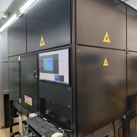
Ultra-short pulse laser micromachining system for semiconductors - Processing trial
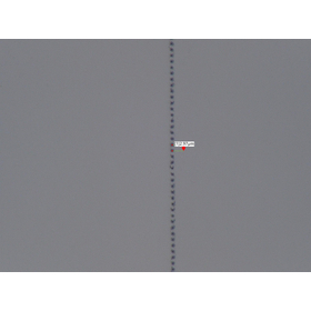
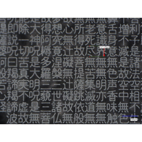
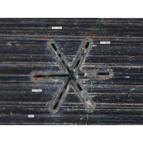
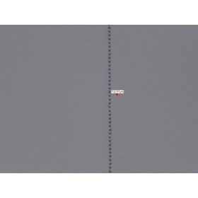
Preliminary verification of fine wiring processing for difficult-to-process materials. Support for laser processing trials.
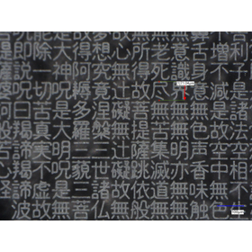
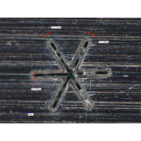
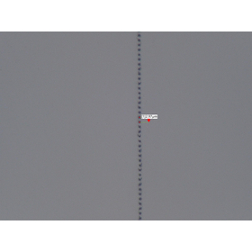
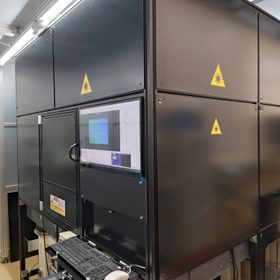
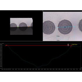
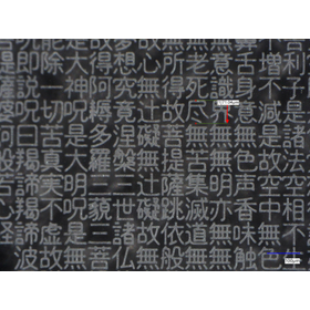
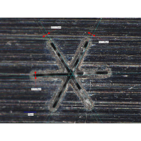
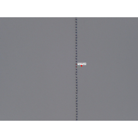
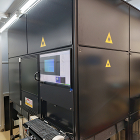
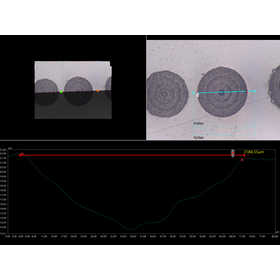
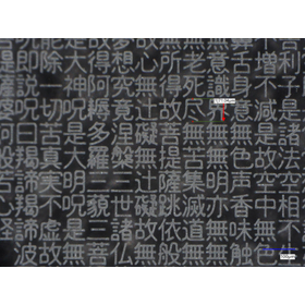
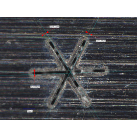
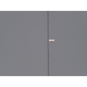
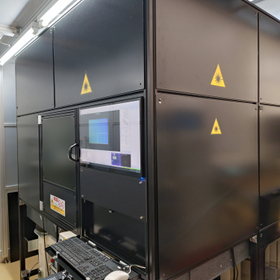
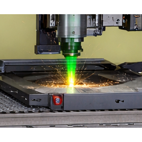
In the semiconductor industry, high-precision processing of fine wiring is directly linked to product performance. In particular, conventional processing methods may raise concerns about cracks and material damage due to thermal effects. To address these challenges and advance the development of reliable products, technologies that achieve precise processing while minimizing the impact on materials are required. NST's ultrashort pulse laser microprocessing system enables high-precision microprocessing while suppressing thermal effects on materials using femtosecond and picosecond level lasers, supporting our customers' technological innovations. 【Application Scenarios】 - Fine wiring processing on silicon wafers - Processing of high-density mounting substrates - Processing verification of next-generation semiconductor materials 【Benefits of Implementation】 - Improved processing accuracy - Reduced damage to materials - Shortened development lead time
- Company:エヌエスティー
- Price:Other